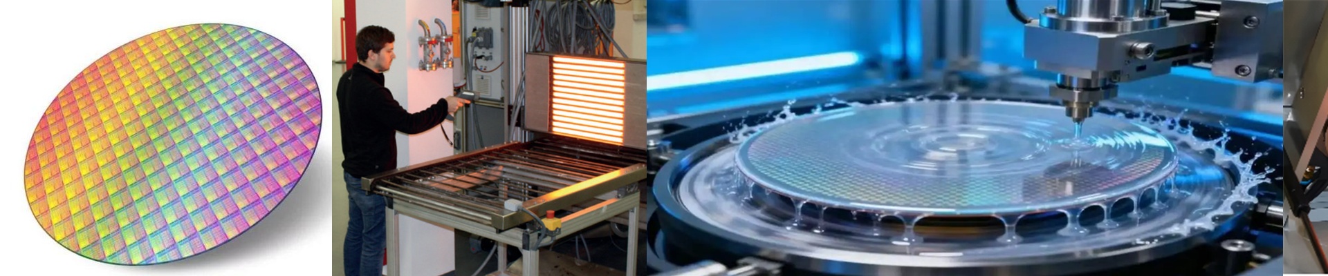
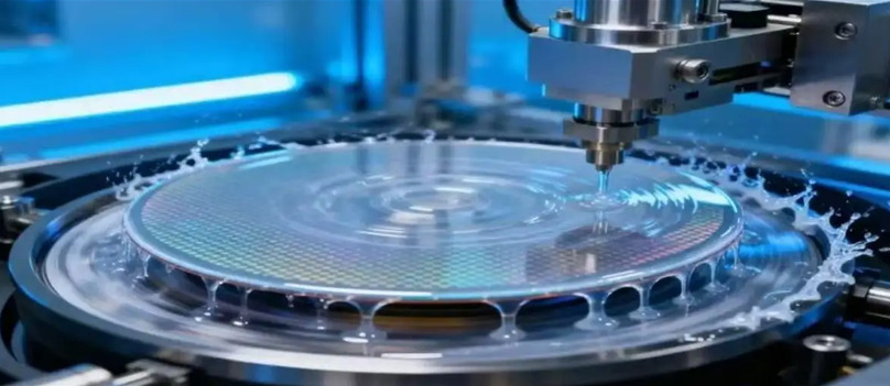
On the fab floor, a 0.5°C drift during the photoresist bake is all it takes to scrap a 300mm wafer. Thermal control isn’t a background task—it’s the boundary the process lives on. We built our NIR heating platform to hold wafer-level uniformity at ±0.1°C, so critical dimensions stay in spec through soft bake and hard bake. What matters under the hood We use near-infrared (NIR) radiant sources paired with fast-response carbon fiber elements, so you get rapid ramp rates without overshoot. Closed-loop control keeps temperature stable across the wafer, even when the soak window runs under a minute. Cleanroom behavior is baked into the design: low outgassing materials, filtered air paths, and surfaces that don’t add particles during operation. You get bake profiles that repeat, shift after shift, and energy use that tracks to cycle time, not to waste heat. Why this matters where you run it In lithography and photoresist processing, temperature uniformity is what sets CD and profile repeatability. Our NIR heaters align with the thermal budget of advanced nodes, giving you tighter control over line-edge roughness and fewer reworks. The upshot is fewer excursions, stable yield, and uptime you can count on. For packaging lines, that same precision translates to consistent cure and solid bond integrity—scrap and rework take a hit. What you need to plan for The platform meets international semiconductor equipment standards and fits existing tool footprints, but integration still needs attention to cleanroom class, exhaust routing, and power conditioning. Expect a short commissioning window to tune your recipe parameters; once those are set, the system runs with minimal adjustment.