
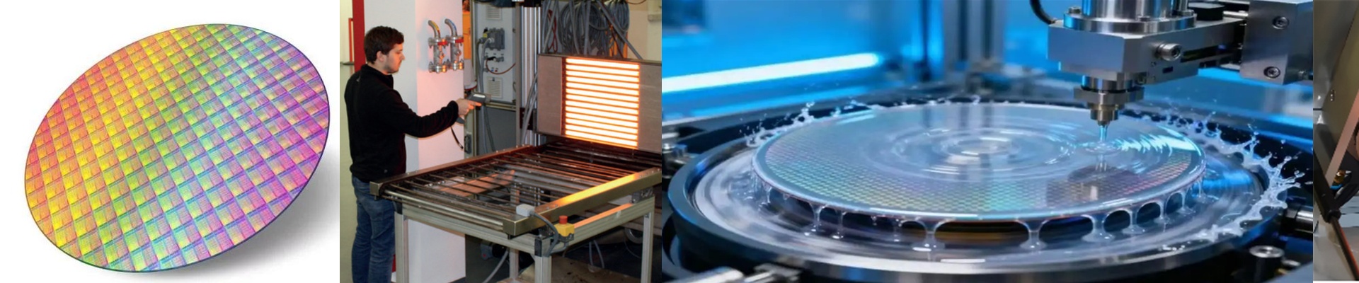
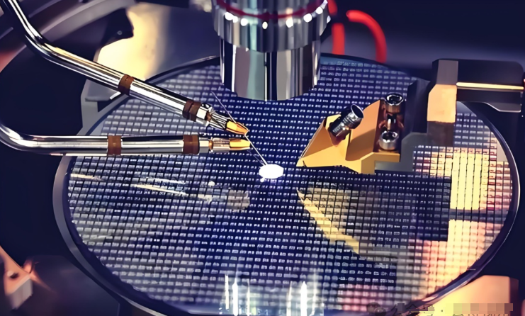
On the fab floor, thermal budget isn’t a suggestion—it’s the line we can’t cross. A few degrees off during photoresist processing and critical dimensions drift after etch. Yield takes the hit, right away. So we built a thermocouple for semiconductor heaters to pull that uncertainty out of every bake step. What matters, technically, is the match. We spec a high-response thermocouple that fits the heater geometry, giving wafer-level thermal uniformity within ±0.1°C across the chuck. The sensor is packaged for cleanroom Class 1–100, with materials chosen to keep outgassing and particle generation low. Repeatability is baked into the calibration curve. Every soft bake and hard bake lands on the same thermal profile, run after run. Response time is tuned for fast stabilization, so the thermal loop stays tight during lithography bake sequences. In lithography, the soft bake pulls solvent out and sets film stress. The hard bake gets the resist ready to stand up to etch and implant. With this thermocouple, you get stable, repeatable temperature control right at the wafer surface—CD control and line-edge roughness stay in spec. That means fewer rework lots, predictable etch selectivity, and device performance that doesn’t wander. Energy use drops, too, because the control loop isn’t chasing overshoot and undershoot. A couple of practical points. Installation needs precise positioning relative to the heater and wafer plane—misalign a millimeter and the measured-to-wafer delta shifts. Match the connector interface and grounding practices to your equipment to keep EMI-induced noise out of the signal. And plan the calibration schedule. Drift is small, but it’s measurable over thousands of cycles. A periodic offset check keeps the process inside the thermal budget where it needs to be.